What is wafer backgrinding? This process involves reducing the thickness of a wafer to allow for high-density packaging of integrated circuits. Backgrinding is the first step in semiconductor device fabrication. After wafer backgrinding, the thinnest wafers will be used to make a transistor. The following article will discuss backgrinding and its benefits. It will also outline the different types of processes used to grind wafers.
Die strength measurements for wafer grinding
The die strength measurements used for wafer grinding have several limitations. First, they are difficult to determine the true strength of the dies. Second, the scatter in the data is large. Third, it is difficult to differentiate between the effects of surface grinding and edge dicing. Further, the geometry of deep scratches influences the die strength measurement. This makes the die strength measurements of IC manufacturing critical. However, this study is a valuable step toward improved testing methods.
Lastly, the abrasive members used in IC manufacturing have various strengths. For example, the maximum die strength was 2,364 MPa, while the lowest value was 998 MPa. A third type of die grinding method uses a ball-rupturing test. In this method, a wafer is in vestigated on different areas before grinding.
The second test method for die strength evaluation is a three-point bending test. This test involves applying three points of force to a silicon die under varying conditions. The three-point bending method has a similar approach, but requires beam-type geometry. However, this technique is not ideal for ultra-thin dies because they have increased flexibility.
The shear fracture strength of the bonded-silicon dies is between 32.8 and 94.4 MPa. The die shear fracture strength of a Sn-Al substrate is dependent on the bonding interface. Die shear strength should be between 32.8 and 97.4 MPa for the manufacturing of wafer-level MEMS packages. If the die shear fracture strength is less than this, the die is not practical.
The ridge-frame structure of the die is observed in Figure 10b. The observer places are labeled “A” to “C” and labeled “Corner”. Position A is near the front surface and shows the largest tensile stress, while position B is near the rear side. The outer bottom corner shows a high tensile stress, which is equivalent to 1.5 GPa.
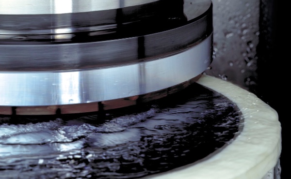
Processes that produce thinner wafers
Thinner wafers are the most efficient way to manufacture semiconductor devices. The technology requires less silicon, which makes the semiconductors thinner. In addition, the thinner wafers also offer more geometrical benefits for packaging. IR is now producing ultra-thin wafers at a diameter of 200 mm. In this paper, we will discuss the thinning process at IR. This process can produce eight to ten new silicon wafers with a thickness tolerance of 20 micrometers.
There are four primary methods of producing thinner semiconductors. However, in some cases, the thinnest wafers are too delicate to hold. They can suffer from microfractures and breakage during the process.
These temporary carriers must be lightweight and resistant to flexure stress. In addition, they must be capable of supporting the device wafer in order to avoid cracking and detachment. These are just a few of the steps that will be involved in the thinning process.
The thinning process involves grinding the wafer up to a final thickness of 70 or 50 um. The back grinding is a critical step in thinning. There are three main stages of back grinding: coarse grind, fine grind, and ultrafine grind. Coarse grind removes silicon faster while fine grind uses smaller diamond particles to reduce the damage to the wafer. The fine grind is often combined with a polishing step to remove any remaining damage layer.
Thermal slide debonding is another technique that involves separating the carrier and device wafer. The wafers slide apart from each other. This process is costly and involves a secondary support mechanism. This secondary support mechanism requires additional machining and adds to the complexity of the process. However, this method is effective in producing thinner wafers than other conventional methods.
In order to manufacture higher quality semiconductors, photovoltaic manufacturers must have innovative core technology. In the U.S., the kerfless direct wafer process is one such example. It also produces thin kerfless wafers with a unique target geometry. Thin interior regions and thick border regions determine the efficiency of the final product.
Thermal transfer and thermal rebonding are two methods that can be used to process thin device wafers. The thermal transfer method relies on the application of a thermoplastic, modified tackified adhesive sheet. This technology allows for a higher volume by minimizing the contact area. However, it is a temporary adhesive and thus has two major drawbacks. The primary material adhesive sheet softens with increasing processing temperature. Also, it releases prematurely.
Click here to read more: https://www.stealthdicing.com/about-gdsi/
Relative risk of defects occurring in wafers
The relative risk of defects occurring in a wafer during grinding is determined by the process used to grind it. A silicon wafer is a flat sheet of silicon with a crystallographic orientation of 100 and a thickness of 500 mm. It is used as a substrate for conductors and semiconductor materials. Grinding a silicon wafer also exposes the surface to additional risks.
The ability to accurately determine the size and location of defects is key to successful semiconductor manufacturing. This process requires rapid development of defect metrology tools and process technology. Historical defect metrology tools simply counted the defects on a characterized wafer, without considering the attributes of the defects. In addition, characterized wafers degrade after multiple tool passes, requiring periodic characterisation of new samples.
The reduction of the Si layer thickness had no effect on Cu retention, but the presence of backside defects improved refresh time. The presence of enough backside defects is critical because it serves as a trapping site for Cu diffusion. If there are not enough backside defects, Cu diffusion may occur, resulting in contamination. A poor gettering ability of the CMP finished surface may cause Cu contamination.
The optimum grind process results in an average wafer thickness of four millimeters, with the difference between the initial and final thickness only varying by 0.5%. This variation in thickness can lead to chucking problems in the tools. This criterion requires a vacuum process tool with a thickness of less than 300 mm. Besides the Si substrate, a silicon wafer may contain molded resin or other materials.
Optical detection systems can also be used to detect defects on nonpatterned wafers. Optical systems that use sub-100 nm sensitivity are based on similar operating principles as those used in larger-scale defect detection. They use DUV illumination-enhanced optical systems. This technique requires high-precision and repeatability in the motion control of the wafer stage.
Choosing the right bevel angle can also reduce the risk of cracks during thinning. The bevel angle of a wafer must fall within the defined SEMI M1-0707 template. A sharper edge is undesirable. The shortest bevel angle is 50 deg for the device area and twenty to thirty degrees for the area removed during thinning.
The relative risk of defects occurring in a wafer depends on the amount of silicon present. A single silicon wafer can have between one and five millimeters of TSV interconnects. The process also depends on the thickness of the device layer and the adhesive. The density of a TSV interconnect is 106 to 107/cm2, and is ten to one hundred times larger than that of a bump interconnect.
Thanks for visiting jetposting